
Research – ultrafast dynamics
Introduction
Generation and detection of terahertz (THz) pulses is achieved using ultrashort laser pulses. The time synchronization of THz and optical pulses makes it naturally possible to perform optical pump—terahertz probe experiments where the optical pulses are used for photoexcitation and the THz pulses are used to probe photo-induced phenomena. In this way, it is possible to study e.g. photoconductivity in semiconductors, response of photoinduced plasma or solvation dynamics. Optical pump—terahertz probe experiments allow achieving a resolution comparable to the laser pulse length, i.e., 10−13 s in our case.
Note also that the process of THz pulse generation (e.g. in photoexcited semiconductors) involves ultrafast photoinduced processes. By a direct inspection of the time profile of the emitted THz pulse, it is possible to learn about the ultrafast dynamics of charge carriers e.g. in semiconductors or in metals (see THz emission spectroscopy).
Ultrafast response of materials is essential for design of fast optoelectronic elements such as modulators, photoswitches, photodetectors or terahertz emitters. For example, opto-THz modulators with modulation speeds up to 1010 bits/s can be conceived and demonstrated.
Our major achievements
- Investigation of electron localization in CdS nanocrystals [1]
- Discovery of the role of electron-cation interaction in dye-sensitized semiconductor nanoparticles [2]
- Interpretation of transient conductivity spectra of free carriers localized in semiconductor nanoparticles [3–6]
- Investigation of ultrafast conductivity in a polymer [7, 8]
- Development of analytical methods for extraction of ultrafast far-infrared response from optical pump—THz probe experiments [9–12].
- Ultrafast opto-terahertz modulators based on photonic crystals [13, 14]
- Investigation of carrier dynamics in semiconductors (microcrystalline silicon, Br+-bombarded InP and InGaAs, GaAs, low-temperature-grown GaAs) [11, 15–20]
- Dynamics of non-resonantly induced plasma in gases [21, 22]
- Terahertz emission due to optical rectification at metal surfaces [23, 24]
Contents
- Electron localization in CdS nanocrystals
- Electron-cation interaction in dye-sensitized ZnO and TiO2 nanocrystals
- Transient conductivity spectra of free carriers localized in semiconductor nanoparticles
- Ultrafast conductivity in a polymer
- Methodology of optical pump—THz probe experiments
- Ultrafast opto-terahertz modulators
- Investigation of carrier dynamics in semiconductors
- Dynamics of non-resonantly induced plasma in gases
- Optical rectification at metal surfaces
Electron localization in CdS nanocrystals
Semiconductor nanocrystals exhibit a plethora of new electronic and optical phenomena owing to their increased surface to volume ratio and carrier confinement. However, the absence of a long-range crystal order fundamentally complicates the charge transport in nanocrystalline films. The underlying physics is very complex as it involves a chain of processes occurring on several different space and time scales.
We have investigated nanocrystalline films of cadmium sulfide (CdS) prepared by chemical bath deposition. In particular, we wish to contribute to the discussion of the long-lasting controversy that nanocrystalline films show the quantum confinement of charges, which is clearly apparent in the optical absorption and emission spectra, and, simultaneously, a long-range bulk-like transport in the electrical measurements. Results obtained by time-resolved terahertz (THz) spectroscopy lead to the following major conclusions:
- Two length scales (nanocrystals and their clusters) control electron localization on the nanoscale
- Electrons with high excess energy have higher mobility than electrons with low excess energy
- The reduced mobility of electrons with low excess energy seems to originate from Coulombic interaction of electron with a localized hole
The spectra of transient conductivity in the THz spectral range are directly related to the nanostructure of the films (Fig. 1a). Firstly, electron localization in nanocrystals leads to a capacitive response characterized by an increasing real part of conductivity and negative imaginary part [1]. By a more detailed inspection we realize that the measured real part is concave above at least 0.4 THz (Fig. 1b) – this is a signature that there is a second length scale of electron localization, which we attribute to nanocrystal clusters seen in Fig. 1a [6]. A more detailed analysis based on Monte-Carlo calculations of conductivity spectra then allows quantitative determination of parameters of electron transport (Fig. 1c). Namely, we found that the probability of electron transport between NCs is rather high (~34%) which shows that the NCs within the cluster are closely packed together. Conversely, the probability of electron transport between NC clusters is much lower (~3%) which indicates that there is much lower contact area between NC clusters as these form a network filled by air pores.
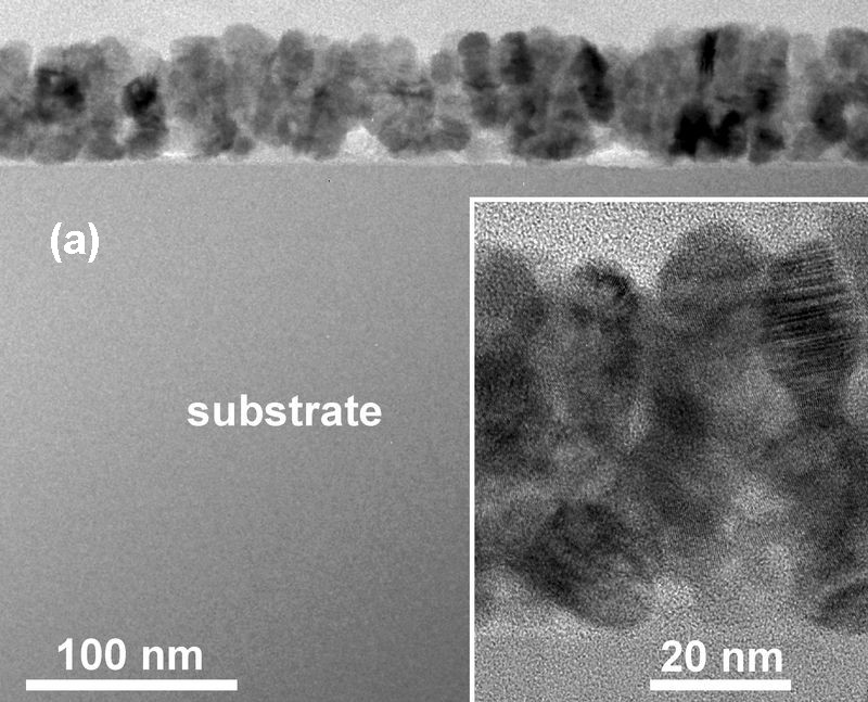
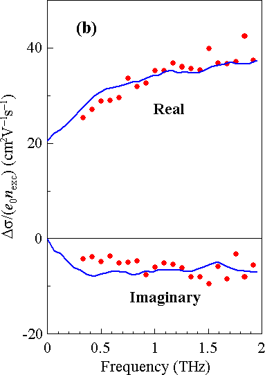
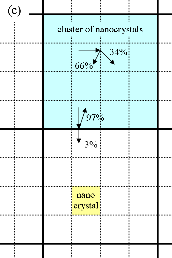
Fig. 1. (a) Transmission-electron-microscope (TEM) image of the cross-section of a CdS film prepared by chemical bath deposition. (b) Example of normalized transient conductivity spectrum (excitation wavelength: 400 nm, pump-probe delay: 10 ps, excitation density: 0.58 photons/NC). Symbols: measured data, lines: calculations by Monte Carlo method [6]. (c) Scheme of the electron transport in the CdS nanocrystalline film (parameters shown are for electrons with low excess energy).
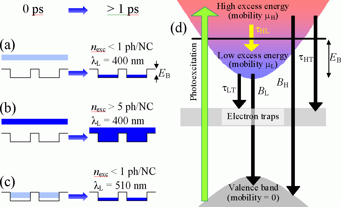

Fig. 2. (a), (b), (c) Schemes illustrating the occupancy of the conduction-band states after photoexcitation (0 ps) and after the subsequent energy relaxation process (>1 ps) for various experimental conditions. (d) Scheme of the kinetic model of electron energy and mobility relaxation, trapping and recombination. (e) Time-dependent THz conductivities (curves are horizontally shifted for clarity; the signal rise for each curve corresponds to the pump-probe overlap). Symbols: measured data, lines: results of fits with kinetic model.
The last question concerns the origin of the potential barriers EB which hinder the motion of electrons with low excess energy and which are not felt by electrons with the high excess energy. We believe that this barrier has a Coulombic origin, i.e., that a hole localized in one NC prevents the electron to escape to another NC. Indeed, the energy required to move an electron from the nanoparticle surface to infinity (when the hole is in the center of the NC) is
| (1) |
for NC radius r = 5 nm and CdS permittivity ε = 9. The estimated value is thus in a perfect agreement with the experimental result EB = 33 meV. Furthermore, this expression predicts that the barrier energy should decrease with increasing NC radius, which is also confirmed by experiment. Finally, let’s note that a Coulombic interaction with a positive charge responsible for reduction of electron mobility was observed in dye-sensitized ZnO nanoparticles [2].
Electron-cation interaction in dye-sensitized ZnO and TiO2 nanocrystals
Dye-sensitized semiconductors are promising materials for applications in solar photovoltaic cells (so-called Grätzel cells). Their operation relies on a cascade of complex physical processes. Here we are interested in processes occurring on the sub-nanosecond time scale which include namely the electron injection into the semiconductor and the initial phase of the electron transport towards the anode. An inefficient electron injection or enhanced electron recombination (due to the slow transport) substantially limits the efficiency of Grätzel cells. Understanding of these phenomena is thus essential for the development of efficient Grätzel cells.
We have investigated systems based on either TiO2 or ZnO nanoparticles. TiO2 is a material commonly used in the Grätzel cells whereas ZnO is intensively studied due to its ability to form easily nanostructures with a wide range of morphologies. The semiconductors were sensitized either by rigid-rod zinc-porphyrins (from the group of Elena Galoppini) or by the commonly used Ru-N3 dye.

Fig. 3.
Left panel. Scheme of a Grätzel cell. Incident radiation first excites dye molecules. Subsequently, the electron (e−) is injected into the semiconductor nanoparticles and it is transported to the electrode. The remaining oxidized dye cation (D+) is reduced by redox electrolyte. Right panel. In TiO2, an electron is injected to the semiconductor nanoparticle in less then 1 ps after photoexcitation. After injection, the electron is free to diffuse through the nanoparticle network to the electrode. In contrast, injection into ZnO occurs via an intermediate electron-cation complex in which the electron and cation are strongly bound to each other. This state is formed within 5 ps and it breaks within 100 ps. After that, the electron is released, but it remains weakly attracted by the cation which makes its transport to the electrode much slower.
Transient conductivity spectra of free carriers localized in semiconductor nanoparticles
Response of charge carriers in bulk semiconductors is in a vast majority of cases described by a Drude model. The conductivity spectra then exhibit two prominent properties: the real part decreases with frequency and the imaginary part is positive. However, the conductivity observed in small semiconductor nanoparticles often behaves differently: it is characterized by a real part increasing with frequency and a negative imaginary part. Such a spectrum can be explained in terms of local field effects provided the nanoparticle size is much larger than the mean free path of charge carriers.
For nanoparticles with size smaller or comparable to the carrier mean free path it is necessary to consider the interaction of carriers with nanoparticle boundaries [6]. Two major effects occur with certain probabilities: (1) the carrier is randomly scattered by the boundary and it may enter another nanoparticle, or (2) it is reflected back and it does not leave the original nanoparticle. In our work we model the thermal motion of carriers inside the nanoparticles and their interaction with the nanoparticle boundary using a Monte Carlo method. The response (i.e. mobility) of carriers is then calculated using the Kubo formula.
Examples of mobilities calculated for an array of perfectly isolated nanospheres are illustrated in Fig. 4. The mobility of carriers always approaches zero for sufficiently low frequencies since there is no path for long-range transport. The real part of mobility shows a peak which shifts to higher frequencies with decreasing ratio of nanoparticle diameter d and carrier mean free path lfree; its frequency represents the mean carrier round-trip frequency in the nanospheres.
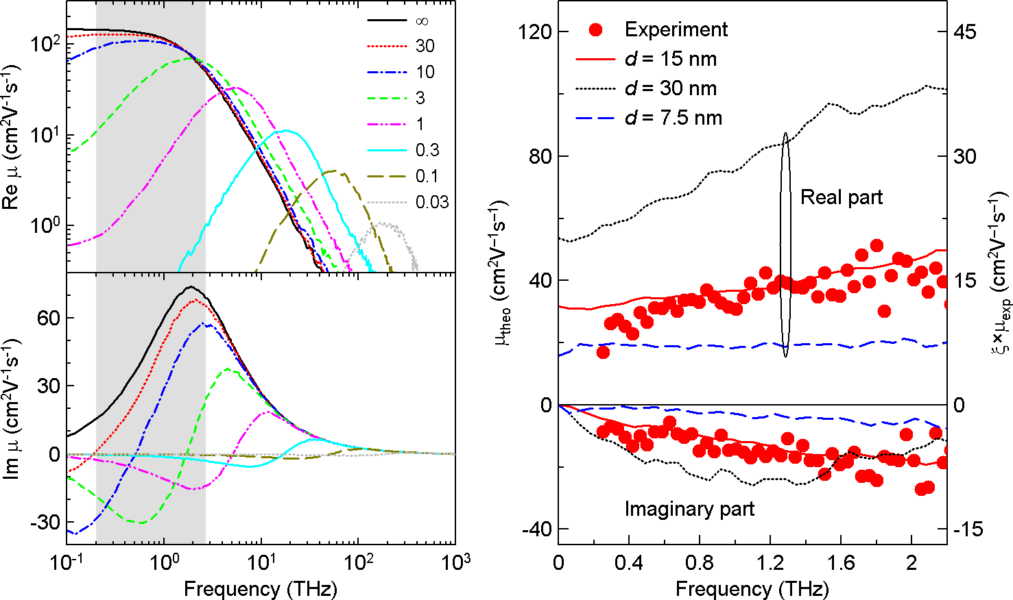
Fig. 4.
Left panel. Spectra of mobility μ in an array of isolated nanospheres calculated using the Monte Carlo method. The mean free path in the bulk was 10 nm and the thermal velocity of carriers was 1.2×10⁵ m/s. The spectra were calculated for ratios of particle diameter d and carrier mean free path lfree in the range of 0.03 and 30 (see the legend). The infinite ratio (d >> lfree) denotes the case where the spectrum approaches the classical Drude model. Right panel. Mobility spectrum of 15-nm ZnO nanoparticles. Points – spectrum measured by time-resolved THz spectroscopy; lines – Monte-Carlo calculations. The lines for other values of d indicate how the spectrum shape would differ if the nanoparticle size were different.
Ultrafast conductivity in a polymer
Materials based on conjugated organic semiconductors are extensively explored in view of promising application, for instance, in inexpensive solar cells. Incident photons first create excitons on polymer chains. In the presence of an acceptor, the excitons rapidly dissociate and a free hole is left on the polymer chain (Fig. 5). One of the unresolved questions concerns the nature of the early stages of the hole transport. Using transient THz spectroscopy, it is possible to characterize conductivity and transport mechanisms in a non-contact manner, on sub-picosecond time scale and using low probing electric fields.
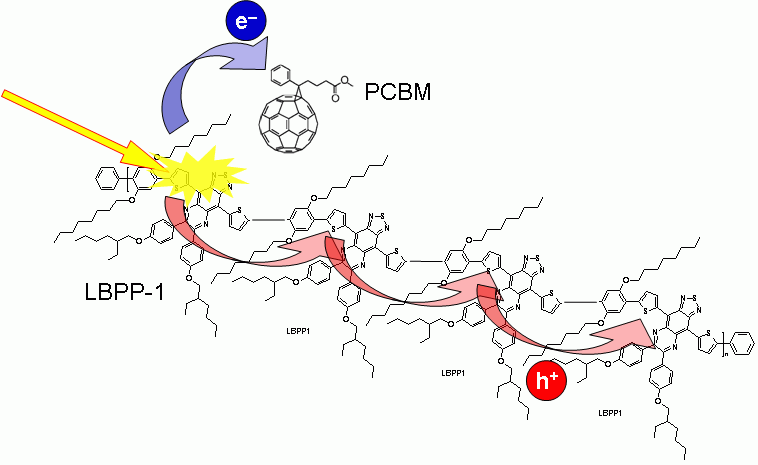
Fig. 5.
Schematics of early photo-initiated processes in polymer:electron-acceptor blends.
We have investigated a blend of a low-band-gap phenylene co-polymer LBPP-1 [Adv. Mater. 19, 3308 (2007)] and a standard electron acceptor PCBM [J. Org. Chem. 60, 532 (1995)]. We show that free holes generated upon photoexcitation of the blend exhibit a very high initial mobility as their initial excess energy facilitates their transport over defects (potential barriers) on polymer chains. The conductivity then drops down rapidly within 1 ps (Fig. 6a), and we demonstrate that this decrease occurs essentially by two mechanisms. First, the carriers lose their excess energy and they thus become progressively localized between the on-chain potential barriers—this results in a mobility decay with a rate of (180 fs−1). Second, carriers are trapped at defects (potential wells) with a capture rate of (860 fs)−1. At longer time scales, populations of mobile and trapped holes reach a quasi-equilibrium state and further conductivity decrease becomes very slow [7].
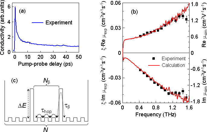
Fig. 6.
(a) Average transient THz conductivity as a function of the time after photoexcitation. (b) Measured and calculated mobility of holes in the LBPP-1:PCBM blend. (c) Scheme of the hole motion along the polymer chain.
Transient THz conductivity spectra measured 2.5 ps after photoexcitation are shown in Fig. 6b. From their shape we conclude that hole transport is essentially controlled by potential barrier on the polymer chains. The model is illustrated in Fig. 6c. The hole can hop between neighboring repeat units and the mean time for this hop is τhop. On the chains, there are potential barriers which are seldom traversed by the holes (with a mean time τβ >> τhop): the barriers enclose Nβ repeat units. The polymer chains are finite and they consist of N repeat units. The mobility spectra were then calculated using a Monte-Carlo method and Kubo formula [7]. A good match with experimental data is found for τhop = 22 fs, τβ = 1.9 ps, and Nβ = 4. The last number indicates that the LBPP-1 chains necessarily contain a high density of defects. It is also possible to estimate that the barrier height ΔE is ~ 120 meV.
Methodology of optical pump—THz probe experiments
Optical pump—THz probe spectroscopy is a way to characterize the non-equilibrium response function which can be represented either by transient conductivity Δσ, or equivalently, by transient susceptibility Δχ. The response function now depends on two variables: on the probing frequency f, and on the delay τp between the excitation and probing pulse.
The experimental arrangement inherits from the setup for THz transmission spectroscopy. There is an extra optical branch which serves to excite the sample (see Fig. 7); the excitation wavelength is often tuned by using wavelength conversion techniques. The time delay τp between the sample excitation and the arrival of the probe pulse is controlled using an additional delay line DL2. The aim of the experiment is the measurement of the change in the THz waveform ΔE(τ, τp) induced by the excitation pulse. The objective is then to extract the transient conductivity Δσ or the transient susceptibility Δχ from the measured data ΔE(τ, τp).
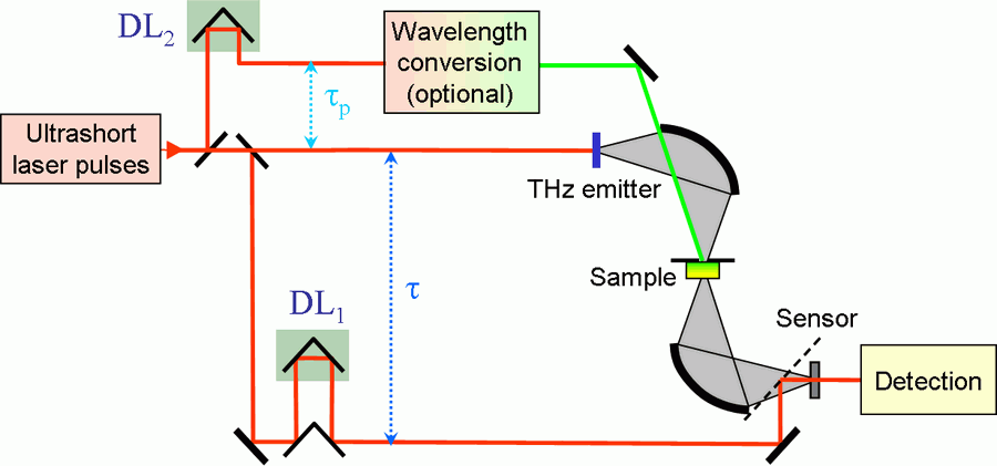
Fig. 7.
Scheme of the optical pump—THz probe experiment. The delay line DL1 controls the gating pulse arrival and its scanning allows measuring the transient THz waveform. The delay line DL2 controls the time of the excitation pulse arrival and its adjustment sets the pump-probe delay τp.
For processes slower than the THz pulse length, we can neglect the change of the state of the sample during the probing event. This means that a so-called quasi-steady-state approximation applies and standard methods for retrieval of optical properties from the measured waveforms can be employed (cf. time-domain THz transmission spectroscopy). However, if we wish to resolve sub-picosecond processes we deal with the situation where the state of the sample is changed on a time scale comparable to (or faster than) the probing event (the probing pulse is typically longer than ~1 ps). In this case, the frequency of the incident radiation is modified: the origin of this phenomenon is demonstrated in Fig. 8. Note that the slower are the investigated processes, the smaller change in frequency may occur. In other words, for slow-enough processes the change in the frequency cannot be resolved and the quasi-steady-state approximation applies.
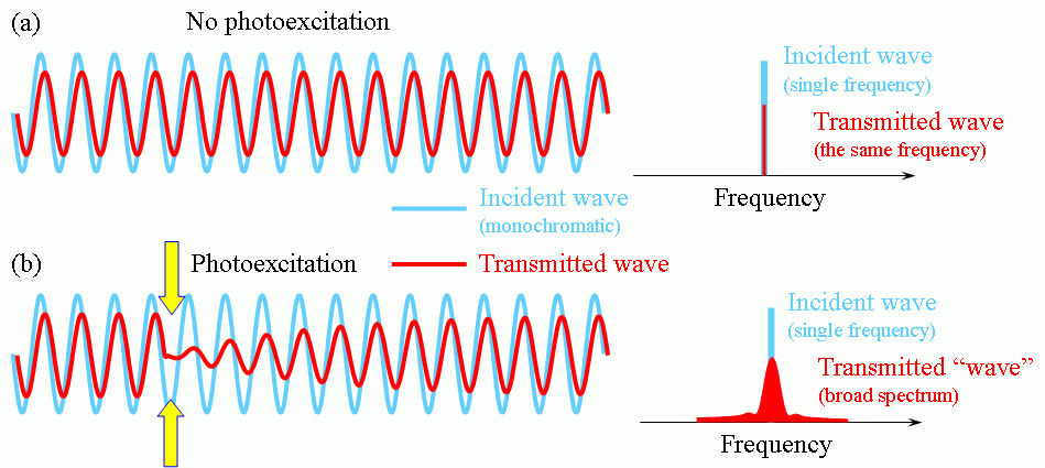
Fig. 8.
Origin of frequency mixing in optical pump—THz probe experiments. (a) Without photoexcitation, the transmitted wave has a smaller amplitude than the incident wave, but the wave frequency is conserved. (b) Upon photoexcitation, the sample (e.g. a semiconductor) becomes opaque and the transmitted wave drops to zero. Later on, the transparency of the semiconductor recovers. The spectrum of the transmitted wave now contains additional components: the so-called frequency mixing occurs.
In Ref. 12 we have shown that the frequency mixing can be elegantly accounted for in the two-dimensional frequency domain. This means, that the delay τ (related to the profile of the THz pulse) is transformed to the frequency f corresponding to the incident spectral components, and simultaneously, the pump-probe delay τp is transformed to the frequency fp which describes the dynamical response of the investigated system. Providing the photo-induced changes are weak, there is a very simple relation between the photo-induced change of the THz waveform ΔE and the incident waveform E0:
 |
(2) |
This expression is a key for the determination of the transient response functions Δχ and Δσ from the experimental data. For this purpose, it is necessary to measure the transient THz waveform ΔE, the incident waveform E0 and to determine the transfer function Ξ (it depends on the experimental geometry and on the ground state refractive index of the investigated sample). These steps are described in detail in Refs. 9 and 12.
Once the spectra Δχ(f, fp) or Δσ(f, fp) being determined, it is necessary to have a basis for their interpretation. In Ref. 11 we have developed models describing two elementary situations: Drude-response of free charge carriers with rapidly decaying population, and bound charge carriers oscillating in a harmonic potential. The transient conductivity corresponding to the former model is illustrated in Fig. 9 along with experimentally determined spectra for radiation-damaged silicon on sapphire. Note that some spectral regions in the (f, fp) plane are not accessible.
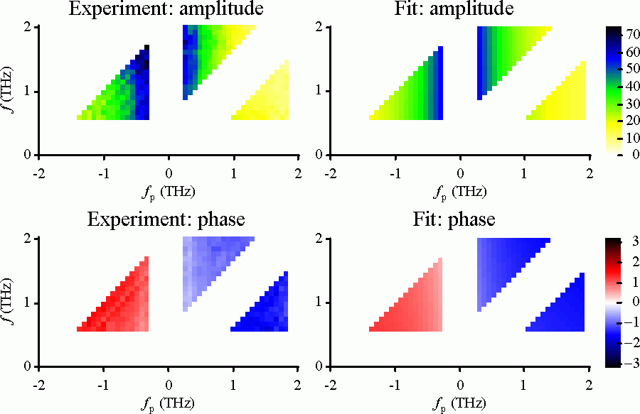
Fig. 9.
Spectra of transient conductivity Δσ of radiation-damaged silicon on sapphire in the two-dimensional frequency domain. Left panels: experimental results, right panels: Drude model of conductivity in the two-dimensional frequency domain. Bottom panels: amplitude of the conductivity |Δσ| in Ω·m−1·THz−1, bottom panels: phase arg(Δσ) in radians. The lifetime of electrons was 420 fs and the electron relaxation time is shorter than 50 fs.
Ultrafast opto-terahertz modulators
Terahertz technology is a research field which has a growing impact e.g. on medical, space and defence industries. As future short-range indoor communication systems may be designed for the sub-terahertz or terahertz range, one can expect a growing emphasis put on the manipulation of both guided and freely propagating terahertz beams by means of agile switches, modulators, and phase shifters controlled either optically or electronically. Optically controlled terahertz switches or filters are of particular interest as they are in principle able to achieve ultrahigh speeds.
High-resistivity semiconductors show a big potential for opto-terahertz coupling. In the ground state, they are transparent and dispersion free for terahertz radiation. Upon optical illumination, free carriers are generated: they exhibit a strong interaction with terahertz radiation, which can be tuned by the illumination.
We have demonstrated that photoexcitation of teh surface of bare GaAs can lead to the tuning of the THz reflection between antireflective (R ≅ 3 %) and highly reflective (R ≅ 85 %) regimes, depending on the excitation intensity [25], Fig. 10).
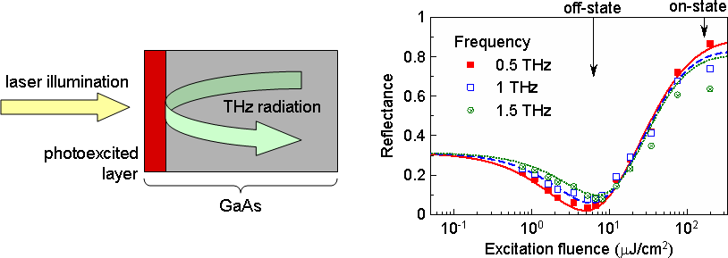
Fig. 10. Left panel: scheme of the opto-terahertz switch based on a photo-excited GaAs wafer with one illuminated surface. Right panel: measured reflectance as a function of excitation fluences for frequencies 0.5, 1.0 and 1.5 THz (the excitation wavelength was 800 nm). Points represent measured data while lines indicate results of modelling.
The use of a bare semiconductor wafer as an opto-terahertz switch is straightforward, but quite high excitation fluences are required for its operation. The controlling excitation fluence can be essentially decreased if the semiconductor is enclosed in a resonant structure—for example, it can play the role of a defect layer in a photonic crystal. In this case, the photonic structure can be designed in such a way that the terahertz electric field is spatially localized in the photo-excited layer, thus enhancing the interaction of the terahertz radiation with the photo-excited semiconductor surface [13, 25]. Such a device is typically narrow-band, since the localization of the electromagnetic field occurs only at the defect-mode frequency. We have shown that the dynamical response is determined by the resonator lifetime (switch-on time) and by the photocarrier lifetime (switch-off time).
An example of the investigated photonic-crystal-based modulator is shown in Fig. 11. It consists of a sequence of alternating layers of quartz and MgO (materials with high contrast of refractive indices at terahertz wavelengths and with high transparency in the visible optical region are required). The device exhibits a response time of ~200 ps, making it possible to construct an opto-terahertz modulator with modulation rates up to 5 GHz.
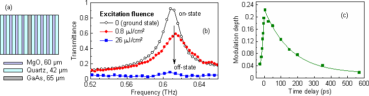
Fig. 11. (a) Scheme of the ultrafast photonic-crystal-based modulator. (b) Measured transmittance spectra for few excitation fluences. A modulation of 50 % can be achieved with excitation fluence as low as 0.8 µJ/cm2. (c) Measured dynamical response of the opto-terahertz modulator at the defect-mode frequency (0.606 THz). The switch-on time is ~20 ps while the switch-off time is ~200 ps and it is limited by the photo-carrier lifetime.
Ultrafast carrier dynamics in semiconductors
Microcrystalline silicon
Microcrystalline silicon is a complex semiconductor material, which drives attention of the companies producing solar cells, displays and other opto-electronics devices. It consists of large grains (hundreds of micrometers) embedded in amorphous silicon tissue (Fig. 12). Large grains are composed of small silicon grains with dimensions of ~20 nm.
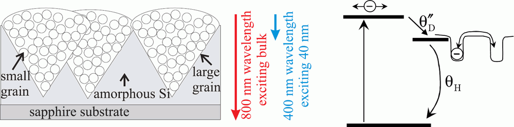
Fig. 12.
Left panel: structure of a microcrystalline silicon on a sapphire substrate. Large grains (~hundred nanometers) have conical shape with a cap and they consist of small grains (~20 nm). Large grains are surrounded by amorphous tissue. Small grains are assumed to be closely packed. Right panel: photoinitiated electron dynamics in microcrystalline silicon.
Using time-resolved THz spectroscopy, we have studied a set of samples with varying crystallinity (0 – 72 %). Two different wavelengths were employed for the photoexcitation: (i) 400 nm which excites only a thin surface layer allows to investigate surface properties, and (ii) 800 nm which creates a homogeneous excitation profile enables to study properties averaged over the entire film thickness. In addition, experiments have been carried out at various temperatures in order to elucidate transport mechanisms of electrons.
The nature of the probing radiation allows us to access local (intra-grain) transport properties. We identified two regimes of conduction. Shortly after photoexcitation, the photogenerated carriers are hot and they exhibit a band-like transport within the small grains. Within θ″D ~ 0.6 ps, the hot carriers fall into shallow states on small grain boundaries (Fig. 12). On longer time scales, these carriers move through hopping between the localized states. Finally, the charge carriers either recombine or become captured in deep traps at large grain boundaries [16, 18].
Ultrafast semiconductors
Photoconductive materials with subpicosecond response times have a wide range of applications in optoelectronics as terahertz emitters, photoswitches, and photodetectors. Their dynamic responsivity depends mainly upon the carrier lifetime, the carrier mobility and the dark resistivity. The group of interesting ultrafast photoconductive materials includes e.g. radiation-damaged silicon-on-sapphire or low-temperature grown GaAs. Short carrier lifetimes are achieved by a generation of a large density of defects either through an ion bombardment or using specific deposition conditions. The corresponding defect energy levels in the band gap then act as carrier traps or recombination centres. The main problem associated with the responsiveness of such materials is that their free-carrier mobility and their resistivity can be significantly reduced comparing to the state without defects. A detailed understanding of the mechanisms of the ultrafast response is thus a crucial point that can allow to optimise the elaboration technology and to control the properties.
Br+-bombarded In0.53Ga0.47As and InP
Particularly interesting optoelectronic properties are produced by bombarding semiconductors by ions with a high initial energy which generates only host-atom displacements near the wafer surface while ions used for the bombardment are implanted a few microns below the wafer surface. Heavy-ion irradiation creates defect clusters in addition to the point defects.
We studied In0.53Ga0.47As and InP irradiated by 11 MeV Br+ ions. Our optical excitation wavelength of 800 nm is absorbed within a sub-micron surface layer. This enabled us to investigate three kinds of samples: (i) bare irradiated InP wafers and (ii) bare irradiated In0.53Ga0.47As films – these contain only host-atom displacements and no implanted Br atoms [B-samples] within the photoexcited layer, and (iii) irradiated InP wafers initially covered with a protective 3 µm-thick In0.47Ga0.53As layer – this layer was etched after irradiation so that we could look into a 3 µm depth where the Br atoms are implanted [E-samples]. Using optical pump—THz probe spectroscopy, we determined the electron trapping times and mobilities as a function of the irradiation dose (Fig. 13). We found that the transport properties are controlled only by the density of host-atom displacements while the Br atom implantation has no significant influence. In the most irradiated sample it was observed that the electron lifetime is as short as 200 fs and that the mobility remains rather high even at the highest irradiation doses [15, 17].
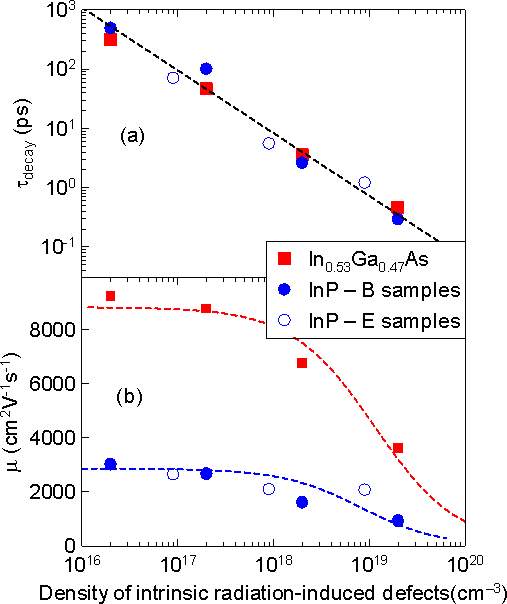
Fig. 13.
Plot of (a) electron trapping time τdecay and (b) of mobility μ as a function of the density of defects resulting from host atom displacements nhost. The dashed line in (a) indicates the trend of the data (τdecay is proportional to 1/nhost), the dashed line in (b) indicates the mobility estimated from a Matthiessen's rule.
Low-temperature-grown GaAs
Using THz emission spectroscopy, we have determined carrier lifetimes and mobilities in a set of samples grown at different temperatures. Sub-picosecond lifetimes and very high mobilities (~2500 cm2V−1sV−1) have been found in all the samples (Fig. 14) [20].
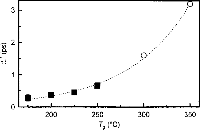
Fig. 14.
Lifetimes of low-temperature-grown GaAs as a function of growth temperature. The empty points were taken from [Appl. Phys. Lett. 70, 2419 (1997)].
Non-linear properties of GaAs
Optical pump–THz probe spectroscopy is also useful for measuring nonlinear optical properties of semiconductors [19]. When amplified pulses at 800 nm illuminate the surface of bulk GaAs, both one- and two-photon excitation of valence electrons occurs and their corresponding concentrations are functions of depth on the scale of several µm. By means of THz probing from inside the sample, it is possible to measure the depth of the photoexcited layer – the method is to a certain extent analogous to time-of-flight spectroscopy. By this method, we have determined, for the first time, the two-photon absorption coefficient β of GaAs at excitation wavelength of ~810 nm.
Dynamics of non-resonantly induced plasma in gases
Another recent extended study using the optical pump—THz probe spectroscopy focused on the mechanism of photoionisation and ultrafast dynamics of the plasma created by photoexcitation in molecular oxygen and nitrogen [21, 22]. We have shown that the ionisation mechanism is multiphoton absorption in case of 400 nm excitation and strong-field effect for the 800 nm pump.
Optical rectification at metal surfaces
Recently, we have demonstrated a new possibility of generating pulsed THz radiation by means of optical rectification at metal surfaces [23, 24]. This phenomenon is due to an effective second-order non-linear susceptibility tensor χijk which vanishes in the bulk of the (centrosymmetric) metals, but is non-zero at the surface and just below due to the absence of translational symmetry. This has been known for decades, as second-harmonic generation at metal surface is well-known. By contrast, optical rectification at metals was not observed until recently. With amplified pulses, we were able to achieve a peak intensity of the electrical field of 4 kV/cm, comparable to that obtained with non-linear crystals.
Related publications
| [1] | Z. Mics, H. Němec, I. Rychetský, P. Kužel, P. Formánek, P. Malý, and P. Němec, Charge transport and localization in nanocrystalline CdS films: a time-resolved terahertz spectroscopy study, Phys. Rev. B 83, 155326 (2011).  |
|---|---|
| [2] | H. Němec, J. Rochford, O. Taratula, E. Galoppini, P. Kužel, T. Polívka, A. Yartsev, and V. Sundström, Influence of the electron-cation interaction on electron mobility in dye-sensitized ZnO and TiO2 nanocrystals: a study using ultrafast terahertz spectroscopy, Phys. Rev. Lett. 104, 197401 (2010). |
| [3] | V. Pushkarev, T. Ostatnický, H. Němec, T. Chlouba, F. Trojánek, P. Malý, M. Zacharias, S. Gutsch, D. Hiller, and P. Kužel, Quantum behavior of terahertz photoconductivity in silicon nanocrystals networks, Phys. Rev. B 95, 125424 (2017). |
| [4] | H. Němec, P. Kužel, and V. Sundström, Charge transport in nanostructured materials for solar energy conversion studied by time-resolved terahertz spectroscopy, J. Photochem. Photobiol. A 215, 123 (2010).  |
| [5] | H. Němec, P. Kužel, F. Kadlec, D. Fattakhova-Rohlfing, J. Szeifert, T. Bein, V. Kalousek, and J. Rathouský, Ultrafast terahertz photoconductivity in nanocrystalline mesoporous TiO2 films, Appl. Phys. Lett. 96, 062103 (2010). |
| [6] | H. Němec, P. Kužel, and V. Sundström, Far-infrared response of free charge carriers localized in semiconductor nanoparticles, Phys. Rev. B 79, 115309 (2009). |
| [7] | H. Němec, H.-K. Nienhuys, E. Perzon, F. Zhang, O. Inganäs, P. Kužel, and V. Sundström, Ultrafast conductivity in a low-band-gap polyphenylene and fullerene blend studied by terahertz spectroscopy, Phys. Rev. B 79, 245326 (2009). |
| [8] | C. Ponseca, H. Němec, N. Vukmirović, S. Fusco, E. Wang, M. Andersson, P. Chábera, A. Yartsev, and V. Sundström, Electron and hole contributions to the terahertz photoconductivity of a conjugated polymer:fullerene blend identified, J. Phys. Chem. Lett. 3, 2442 (2012). |
| [9] | P. Kužel, F. Kadlec, and H. Němec, Propagation of terahertz pulses in photoexcited media: Analytical theory for layered systems, J. Chem. Phys. 127, 024506 (2007). |
| [10] | H. Němec, F. Kadlec, S. Surendran, P. Kužel, and P. Jungwirth, Ultrafast far-infrared dynamics probed by terahertz pulses: A frequency domain approach. I. Model systems, J. Chem. Phys. 122, 104503 (2005). |
| [11] | H. Němec, F. Kadlec, C. Kadlec, P. Kužel, and P. Jungwirth, Ultrafast far-infrared dynamics probed by terahertz pulses: A frequency domain approach. II. Applications, J. Chem. Phys. 122, 104504 (2005). |
| [12] | H. Němec, F. Kadlec, and P. Kužel, Methodology of an optical pump-terahertz probe experiment: An analytical frequency-domain approach, J. Chem. Phys. 117, 8454 (2002). |
| [13] | L. Fekete, F. Kadlec, H. Němec, and P. Kužel, Fast one-dimensional photonic crystal modulators for the terahertz range, Opt. Exp. 15, 8898 (2007). |
| [14] | L. Fekete, F. Kadlec, P. Kužel, and H. Němec, Ultrafast opto-terahertz photonic crystal modulator, Opt. Lett. 32, 680 (2007). |
| [15] | J. C. Delagnes, P. Mounaix, H. Němec, L. Fekete, F. Kadlec, P. Kužel, M. Martin, and J Mangeney, High photocarrier mobility in ultrafast ion-irradiated In0.53Ga0.47As for terahertz applications, J. Phys. D 42, 195103 (2009). |
| [16] | L. Fekete, P. Kužel, H. Němec, F. Kadlec, A. Dejneka, J. Stuchlík, and A. Fejfar, Ultrafast carrier dynamics in microcrystalline silicon probed by time-resolved terahertz spectroscopy, Phys. Rev. B 79, 115306 (2009). |
| [17] | H. Němec, L. Fekete, F. Kadlec, P. Kužel, M. Martin, J. Mangeney, J. C. Delagnes, and P. Mounaix, Ultrafast carrier dynamics in Br+-bombarded InP studied by optical pump — terahertz probe spectroscopy, Phys. Rev. B 78, 235206 (2008). |
| [18] | L. Fekete, H. Němec, F. Kadlec, P. Kužel, J. Stuchlík, A. Fejfar, J. Kočka, Carrier dynamics in microcrystalline silicon studied by time-resolved terahertz spectroscopy, J. Noncryst. Solids 352, 2846 (2006). |
| [19] | F. Kadlec, H. Němec, and P. Kužel, Optical two-photon absorption in GaAs measured by optical-pump terahertz-probe spectroscopy, Phys. Rev. B 70, 125205 (2004). |
| [20] | H. Němec, A. Pashkin, P. Kužel, M. Khazan, S. Schnüll, and I. Wilke, Carrier dynamics in low-temperature grown GaAs studied by terahertz emission spectroscopy, J. Appl. Phys. 90, 1303 (2001). |
| [21] | Z. Mics, P. Kužel, P. Jungwirth, and S. E. Bradforth, Photoionization of atmospheric gases studied by time-resolved terahertz spectroscopy, Chem. Phys. Lett. 465, 20 (2008). |
| [22] | Z. Mics, F. Kadlec, P. Kužel, P. Jungwirth, S. E. Bradforth, V. A. Apkarian, Nonresonant ionization of oxygen molecules by femtosecond pulses: Plasma dynamics studied by time-resolved terahertz spectroscopy, J. Chem. Phys. 123, 104310 (2005). |
| [23] | F. Kadlec, P. Kužel, J.-L. Coutaz, Study of terahertz radiation generated by optical rectification on thin gold films, Opt. Lett. 30, 1402 (2005). |
| [24] | F. Kadlec, P. Kužel, and J.-L. Coutaz, Optical rectification at metal surfaces, Opt. Lett. 29, 2674 (2004). |
| [25] | L. Fekete, J. Y. Hlinka, F. Kadlec, P. Kužel, and P. Mounaix, Active optical control of the terahertz reflectivity of high-resistivity semiconductors, Opt. Lett. 30, 1992 (2005). |
| last change December 13, 2018 | (home page) |
|---|