
News
Microscopic interpretation of THz conductivity spectra
THz spectroscopy is a great tool for investigation of (ultrafast) conductivity of nanostructured materials since it provides a contactless access to the dynamical charge carrier transport phenomena. However, quantitative interpretation of the experimental conductivity spectra beyond the phenomenological level is still a subject of scientific debate.
Formulation of the problem
Nanoscaled materials are inherently inhomogeneous and their macroscopic photoconductive response (as measured by transient terahertz spectroscopy) usually significantly differs from that of bulk materials. The reason of this behavior is in principle twofold:
- The microscopic mobility spectrum μ(ω) of individual charge carriers may show a significant deviation from the Drude-like behavior in the THz spectral range due to their interactions with nanocrystal boundaries. Note that we understand μ(ω) as a charge carrier response function (not to be confused with the dc or drift mobility which is a single value describing a long-range transport), i.e. as a photoconductivity per single unit charge: μ = Δσmic/eN, where N is the density of photocarriers. This mobility describes how the carrier motion is responding to the local field (which the carriers directly “feel” inside nanocrystals).
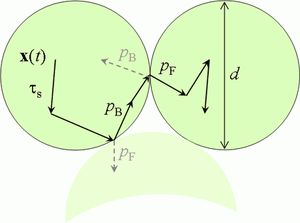
Fig. 1. Carriers scatter in the bulk of nanocrystals but they may also interact with the nanocrystal boundaries. This interaction deeply modify the nature of the charge carrier response function μ(ω). - The macroscopic photoconductivity, which is measured by THz spectroscopy, reflects an effective response of charge carriers to an external (THz) electric field (which may be different from the local one due to depolarization fields). Consequently, the relation between the photoconductivity and the microscopic mobility may be non-trivial and frequently it has a nonlinear character. As a consequence, the spectral shape of the measured conductivity Δσ(ω) may differ from that of the microscopic mobility μ(ω). In particular, THz spectra of carriers in non-percolated inclusions, which are incorporated in an insulating or weakly conducting matrix, show a plasmon resonance due to local depolarization fields.
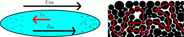
Fig. 2. Carriers scatter in the bulk of nanocrystals but they may also interact with the nanocrystal boundaries. This interaction deeply modify the nature of the charge carrier response function μ(ω).


In our view, the measured spectrum is always a combination of these two effects and, in order to get a microscopic insight into the charge carrier transport and dynamics, one should disentangle these two phenomena. Various groups have been using the Drude-Smith model
 |
(1) |
to fit the experimental conductivity spectra. In our opinion, the direct fitting of the Drude-Smith model to the raw conductivity spectrum may be justified only when the effect of depolarization fields can be neglected (strong percolation, very weak excitation intensities leading to low carrier densities N). In this case a microscopic interpretation of the Drude-Smith parameters is possible [1]. However, if the depolarization fields play an important role in the sample, the Drude-Smith parameters become formal numbers which allow one to reproduce the shape of the spectrum but do not describe the physics behind it.
Analytical description
Recently, we proposed a general analytical description where the carrier transport and depolarizations fields are systematically disentangled for non-percolated samples and for samples with complex percolation pathways [2]. The model consists in three steps.
1st step
We solve the wave equation in an inhomogeneous sample. Note that the inhomogeneity is two-fold: the one due to nanocrystalline structure and the one due to inhomogeneous nature of photoexcitation (excitation decay in the direction perpendicular to the sample surface).

Fig. 3. Scheme of photoexcitation of the sample.
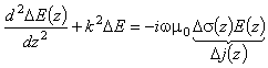
In Fig. 3 Einc is the incident THz radiation, Et is the transmitted THz field without photoexcitation (in equilibrium) and ΔEt is its change due to the photoexcitation represented by the photoconductivity Δσ. Inside the sample (yellow part) the wave equation for the transient field ΔE must be fulfilled:
 |
(2) |
The source right-hand-side term of this equation is the photoinduced current in the THz probing field. It is possible to determine a relation between a measurable quantity (e.g. transient transmission, ΔEt/Et) and the photo-conductivity for any useful experimental geometry [2]. Here we discuss only a specific example of a thin photoexcited film; for this particular case we obtain:
| (3) |
where we introduced a transient sheet conductivity
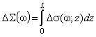 |
(4) |
ΔΣ can be then understood as a directly measured quantity for any spatial profile of the photoconductivity Δσ. Note also, that the conductivity profile can also in principle vary in time, e.g. due to the diffusion of carriers into the bulk of the sample; the theory remains valid.
2nd step
We postulate and justify a relation between the effective photoconductivity Δσ and the microscopic photoconductivity Δσmic [3]:
| (5) |
This so called “VBD” model is parameterized by 3 independent parameters V, B, and D which are completely determined by the sample morphology (they are temperature and carrier density independent). V is the percolation strength and the coefficients B and D describe the conductance and capacitance of the non-percolated part of the sample; D is directly related to the dominant depolarization factor of the structure. We have demonstrated the following properties:
- the VBD model is conform with the Bergman representation of effective medium theory with a single dominant depolarization factor
- the VBD model can also describe the Maxwell-Garnett effective medium model
- the pole in the denominator of (5) describes the localized plasmon resonance in nanoparticles
- extensive 2D electrostatic simulations show that this model describes a large number of morphologies including complex percolation pathways (like red pathway depicted in the right panel of Fig. 2). [3]
Discussion of the shape of transient transmission spectra for the case thick samples (with thick photoexcited layer) and the implications for their interpretation can be found e.g. in [2, 4].
3rd step
The microscopic response function Δσmic = eNμ is determined in the semi-classical limit by Monte-Carlo calculations of the motion charge carriers inside nanoparticles [1]. These calculations make use of the Kubo formula which, for the non-degenerated semiconductors described by the Maxwell-Boltzmann statistics, reads
| (6) |
This formula links the thermal motion of charges through the velocity autocorrelation function to the mobility spectrum.
In the simulations of the thermal motion, we consider forces acting on the charges inside nanoparticles: trajectories of carriers are calculated by numerical solution of Newton’s equations of motion. Furthermore, we describe the interaction of carriers with nanoparticle boundaries. Two major effects occur with certain probabilities: (1) the carrier is randomly scattered at the boundary and it may enter another nanoparticle, or (2) it is reflected back and it does not leave the original nanoparticle (see Fig. 1).
Examples of mobilities calculated for perfectly isolated nanospheres (i.e. only backscattering is allowed at the boundaries) are illustrated in Fig. 4. The mobility of carriers approaches zero for sufficiently low frequencies since there is no path for long-range transport. The real part of the mobility shows a peak which shifts to higher frequencies with decreasing ratio of nanoparticle diameter d and carrier mean free path lfree; its frequency represents the mean carrier round-trip frequency in the nanospheres.

Fig. 4. Spectra of the real (upper panel) and imaginary (lower panel) part of the mobility of a charge carrier enclosed in a perfectly isolated nanosphere. The spectra are plotted for varying ratio d/lfree.
From the upper panel it is obvious that the maximum of the mobility decreases for smaller nanoparticles, and that the peak of the mobility continuously shifts towards higher frequencies. This means that the response dramatically drops down for smaller nanoparticles. This has important consequences for investigation of very small nanocrystals. If the sample is “polluted” by the presence of a small number of large particles, their response may dominate whereas the response of the small nanoparticles may only weakly contribute [4].
Experimental procedure
Equation (5) is introduced into (4) to relate the microscopic conductivity to the measured sheet conductivity. In this way we can fit the microscopic response function to the experimental data which deconvolutes the response (Δσmic, μ) from depolarization fields (V, B, D). To achieve this, we must perform careful experiments versus the excitation density (concentration of photocarriers) over several orders of magnitude. Such experiments may be time consuming because the signal from very weakly photoexcited nanostructures is extremely small.
Related publications
| [1] |
H. Němec, P. Kužel, and V. Sundström,
Far-infrared response of free charge carriers localized in semiconductor nanoparticles,
Phys. Rev. B 79, 11 5309 (2009).

|
|---|---|
| [2] |
P. Kužel and H. Němec,
Terahertz conductivity in nanoscaled systems: effective medium theory aspects,
J. Phys. D: Appl. Phys., 47, 374005 (2014).
|
| [3] |
H. Němec, V. Zajac, I. Rychetský, D. Fattakhova-Rohlfing, B. Mandlmeier, T. Bein, Z. Mics, and P. Kužel,
Charge transport in TiO2 films with complex percolation pathways investigated by time-resolved terahertz spectroscopy,
IEEE T. THz. Science Technol. 3, 302 (2013).
|
| [4] |
V. Zajac, H. Němec, C. Kadlec, K. Kůsová, I. Pelant, and P. Kužel,
THz photoconductivity in light-emitting surface oxidized Si nanocrystals: the role of large particles,
New J. Phys 16, 093013 (2014).
|
| last change 17 December 2015 | (home page) |
|---|