
Výzkum – ultrarychlá dynamika
Úvod
Generování a detekce terahertzových (THz) pulsů je řízena ultrakrátkými laserovými pulsy. Časová synchronizace THz a optických pulsů umožňuje přirozeně realizovat experimenty typu optická excitace—THz sondování, v nichž jsou optické pulsy využity pro fotoexcitaci a THz pulsy sondují fotoindukované procesy. Tímto způsobem je možné studovat např. fotovodivost v polovodičích, odezvu fotoindukovaného plazmatu nebo solvatační dynamiku. Experimenty typu optická excitace—THz sondování umožňují dosáhnout časového rozlišení srovnatelného s délkou laserových pulsů, což je v našem případě 10−13 s.
Uvědomme si, že také procesy generování THz pulsů (např. ve fotoexcitovaných polovodičích) zahrnují ultrarychlé fotoindukované procesy. Přímým pozorováním časového profilu emitovaných THz pulsů tak můžeme získat informaci o ultrarychlé dynamice nosičů náboje, např. v polovodičích nebo v kovech (viz též THz emisní spektroskopie).
Ultrarychlá odezva materiálů je zásadní pro konstrukci rychlých optoelektronických prvků jako jsou modulátory, fotospínače, fotodetektory nebo terahertzové emitory. Dosud byly navrženy a předvedeny například opto-THz modulátory s modulačními rychlostmi až 1010 bits/s.
Naše hlavní výsledky
- Objev významu interakce elektronu a kationu v senzibilizovaných polovodičových nanočásticích [4]
- Interpretace fotovodivostních spekter volných nábojů lokalizovaných v polovodičových nanočásticích [3, 5, 8]
- Studium ultrarychlé vodivosti polymerů [1, 7]
- Vývoj analytických metod pro určování ultrarychlé THz odezvy z experimentů typu optická excitace—THz sondování [13, 19, 20, 24].
- Ultrarychlé opto-terahertzové modulátory založené na fotonických krystalech [12, 14]
- Výzkum dynamiky nosičů náboje v polovodičích (mikrokrystalický křemík, InP a InGaAs bombardovaný ionty Br+, GaAs, GaAs pěstovaný při nízkých teplotách) [6, 9, 10, 15, 20, 22, 25]
- Dynamika nerezonantně indukovaného plazmatu v plynech [11, 16]
- Emise terahertzového záření v důsledku optické rektifikace na povrchu kovů [18, 21]
Obsah
- Interakce elektronu a kationu v senzibilizovaných nanočásticích ZnO a TiO2
- Fotovodivostní spektra volných nábojů lokalizovaných v polovodičových nanočásticích
- Ultrarychlá fotovodivost polymerů
- Metodika experimentů typu optická excitace—THz sondování
- Ultrarychlé opto-terahertzové modulátory
- Výzkum dynamiky nosičů náboje v polovodičích
- Dynamika nerezonantně indukovaného plazmatu v plynech
- Optická rektifikace na povrchu kovů
Interakce elektronu a kationu v senzibilizovaných nanočásticích ZnO a TiO2
Polovodiče senzibilizované molekulami barviva jsou perspektivní materiály pro aplikaci v solárních fotovoltaických článcích (tzv. Grätzelovy články). Jejich funkce je založena na kaskádě složitých fyzikálních procesů. Zde se zajímáme o procesy probíhající na sub-nanosekundové časové škále, které zahrnují zejména injekci elektronu do polovodiče a počáteční fázi transportu elektronu k anodě. Neúčinná injekce elektronu nebo podstatná rekombinace elektronů (v důsledku pomalého transportu elektronů) podstatně snižuje účinnost Grätzelových článků. Porozumění těmto jevům je proto zásadní pro vývoj účinných Grätzelových článků.
Zkoumali jsme systémy založené buď na nanočásticích TiO2 nebo ZnO. TiO2 je materiál standardně používaný v Grätzelových článcích zatímco ZnO je intenzivně studován pro svoji schopnost snadno tvořit nanostruktury s velmi rozmanitými morfologiemi. Polovodiče jsme senzibilizovali buď zinečnatými porfyriny s pevným uchycením (ze skupiny Eleny Galoppini) nebo standardním barvivem Ru-N3.

Obr. 1.
Levá část. Schéma Grätzelova článku. Dopadající záření nejprve excituje molekuly barviva. Následně dochází k injekci elektronu (e−) do polovodičové nanočástice a k jeho transportu k elektrodě. Zbývající kation oxidovaného barviva (D+) je redukován redoxním elektrolytem. Pravá část. V TiO2 je elektron injektován do polovodičové nanočástice za méně než 1 ps po fotoexcitaci. Po injekci je elektron volný a může difundovat skrz systém nanočástic k elektrodě. Naproti tomu injekce do ZnO probíhá přes mezistav (elektron-kationový komplex) ve kterém jsou spolu elektron i kation silně svázány. Tento stav se vytvoří během 5 ps a rozpadne se během 100 ps. Po rozpadu je elektron uvolněn, ale stále zůstává slabě přitahován ke kationu, což výrazně zpomalí jeho transport k elektrodě.
Fotovodivostní spektra volných nábojů lokalizovaných v polovodičových nanočásticích
Odezvu nosičů volných nábojů v objemových polovodičích můžeme v převážné většině případů popsat Drudeho modelem. Taková vodivost má dvě podstatné vlastnosti: klesající reálnou část, a kladnou imaginární část. Naproti tomu vodivostní spektra polovodičových nanočástic jsou často zcela odlišná a bývají charakterizována rostoucí reálnou částí a zápornou imaginární částí. Takové spektrum lze vysvětlit působením lokálních polí v případech, kdy je velikost nanočástic mnohem větší než střední volná dráha nosičů náboje.
Pro nanočástice s velikostí menší nebo srovnatelnou se střední volnou dráhou nosičů náboje je nutné uvažovat interakci nosičů s povrchem nanočástic [8]. S určitou pravděpodobností může dojít ke dvěma hlavním jevům: (1) nosič je na povrchu nanočástice rozptýlen do zcela náhodného směru a může proniknout do sousední nanočástice, nebo (2) nosič se od povrchu nanočástice odrazí a zůstane v původní nanočástici. Zde používáme metodu Monte Carlo s níž simulujeme tepelný pohyb nosičů uvnitř nanočástic a interakci nosičů s povrchem nanočástic. Lineární odezva (např. pohyblivost) je pak vypočtena pomocí Kubovy formule.
Příklady spekter pohyblivosti vypočítaných pro případ zcela izolovaných nanokuliček jsou uvedeny na obr. 2. Spektrum pohyblivosti je při dostatečně nízkých frekvencích vždy nulové, protože neexistuje transport na dlouhou vzdálenost. V reálné část pohyblivosti se nachází maximum, které se posouvá k vyšším frekvencím s klesajícím poměrem průměru nanokuliček d a střední volné dráhy nosičů náboje lfree. Frekvence maxima odpovídá střední době za kterou nosič náboje projde nanokuličkou.
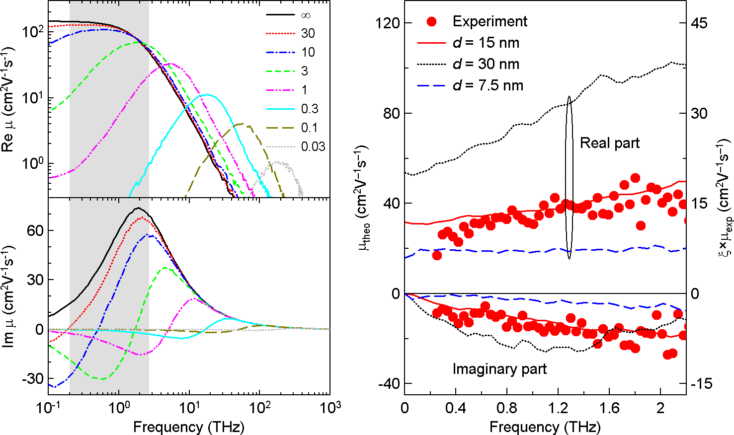
Obr. 2.
Levá část. Spektra pohyblivosti μ v souboru izolovaných nanokuliček, vypočtená s použitím metody Monte Carlo. Střední volná dráha nosičů náboje byla 1.2×10⁵ m/s. Spektra byla vypočtená pro poměry průměrů nanočástic d a středních volných drah lfree v rozmezí od 0.03 do 30 (viz popiska grafu). Nekonečný poměr (d >> lfree) označuje případ, ve kterém spektrum odpovídá klasickému Drudeho modelu. Pravá část. Porovnání pohyblivostních spekter nanočástic ZnO o průměru 15 nm (symboly – změřené metodou časově rozlišené THz spektroskopie) a výsledků simulací Monte Carlo (křivky). Křivky pro další hodnoty d ukazují, jak by se lišila spektra pokud by byl průměr nanočástic odlišný.
Ultrarychlá fotovodivost polymerů
Materiály založené na konjugovaných organických polovodičích jsou intenzivně zkoumány např. z hlediska aplikací v levných solárních článcích. Dopadající fotony nejprve vytvoří excitony na polymerních řetězcích. V přítomnosti akceptoru dojde k velmi rychlé disociaci excitonů a na polymerním řetězci zůstane kladně nabitá díra (obr. 3). Jednou z nevyřešených otázek je mechanismus transportu náboje těsně po vytvoření díry. Časově rozlišená THz spektroskopie umožňuje bezkontaktně charakterizovat vodivost a mechanismy transportu na sub-pikosekundové časové škále a s použitím nízkých elektrických polí.
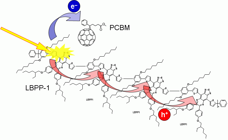
Obr. 3.
Schéma foto-iniciovaných procesů ve směsi polymeru a elektronového akceptoru
Zkoumali jsme směs fenylenového kopolymeru LBPP-1 [Adv. Mater. 19, 3308 (2007)] a standardního elektronového akceptoru PCBM [J. Org. Chem. 60, 532 (1995)]. Ukázali jsme, že volné díry vytvořené po fotoexcitaci směsi jsou velmi pohyblivé, a to v důsledku jejich přebytečné počáteční energie, která usnadňuje jejich transport přes defekty (potenciálové bariéry) na řetězci polymeru. Vodivost potom během 1 ps velmi rychlé klesá (obr. 4a). Ukázali jsme, že tento pokles nastává dvěma mechanismy. Nosiče náboje jednak ztrácejí svoji přebytečnou energii a tím dochází k jejich postupné lokalizaci mezi potenciálovými bariérami na polymerním řetězci: to vede k poklesu pohyblivosti s rychlostí (180 fs−1). Nosiče náboje jsou také zachytávány v defektech (v potenciálových jámách) s rychlostí (860 fs)−1. Na delších časových škálách potom dochází k ustanovování kvazirovnováhy mezi pohyblivými a zachycenými děrami, což vede k podstatnému zpomalení poklesu vodivosti [7].
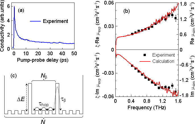
Obr. 4.
(a) Střední THz fotovodivost jako funkce času po fotoexcitaci. (b) Změřená a vypočítaná pohyblivost děr ve směsi LBPP-1:PCBM. (c) Schéma pohybu díry po polymerním řetězci.
Transient THz conductivity spectra measured 2.5 ps after photoexcitation are shown in Fig. 4b. From their shape we conclude that hole transport is essentially controlled by potential barrier on the polymer chains. The model is illustrated in Fig. 4c. The hole can hop between neighboring repeat units and the mean time for this hop is τhop. On the chains, there are potential barriers which are seldom traversed by the holes (with a mean time τβ >> τhop): the barriers enclose Nβ repeat units. The polymer chains are finite and they consist of N repeat units. The mobility spectra were then calculated using a Monte-Carlo method and Kubo formula [7]. A good match with experimental data is found for τhop = 22 fs, τβ = 1.9 ps, and Nβ = 4. The last number indicates that the LBPP-1 chains necessarily contain a high density of defects. It is also possible to estimate that the barrier height ΔE is ~ 120 meV.
Methodology of optical pump—THz probe experiments
Optical pump—THz probe spectroscopy is a way to characterize the non-equilibrium response function which can be represented either by transient conductivity Δσ, or equivalently, by transient susceptibility Δχ. The response function now depends on two variables: on the probing frequency f, and on the delay τp between the excitation and probing pulse.
The experimental arrangement inherits from the setup for THz transmission spectroscopy. There is an extra optical branch which serves to excite the sample (see Fig. 5); the excitation wavelength is often tuned by using wavelength conversion techniques. The time delay τp between the sample excitation and the arrival of the probe pulse is controlled using an additional delay line DL2. The aim of the experiment is the measurement of the change in the THz waveform ΔE(τ, τp) induced by the excitation pulse. The objective is then to extract the transient conductivity Δσ or the transient susceptibility Δχ from the measured data ΔE(τ, τp).
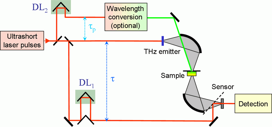
Fig. 5.
Scheme of the optical pump—THz probe experiment. The delay line DL1 controls the gating pulse arrival and its scanning allows measuring the transient THz waveform. The delay line DL2 controls the time of the excitation pulse arrival and its adjustment sets the pump-probe delay τp.
For processes slower than the THz pulse length, we can neglect the change of the state of the sample during the probing event. This means that a so-called quasi-steady-state approximation applies and standard methods for retrieval of optical properties from the measured waveforms can be employed (cf. time-domain THz transmission spectroscopy). However, if we wish to resolve sub-picosecond processes we deal with the situation where the state of the sample is changed on a time scale comparable to (or faster than) the probing event (the probing pulse is typically longer than ~1 ps). In this case, the frequency of the incident radiation is modified: the origin of this phenomenon is demonstrated in Fig. 6. Note that the slower are the investigated processes, the smaller change in frequency may occur. In other words, for slow-enough processes the change in the frequency cannot be resolved and the quasi-steady-state approximation applies.
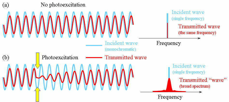
Fig. 6.
Origin of frequency mixing in optical pump—THz probe experiments. (a) Without photoexcitation, the transmitted wave has a smaller amplitude than the incident wave, but the wave frequency is conserved. (b) Upon photoexcitation, the sample (e.g. a semiconductor) becomes opaque and the transmitted wave drops to zero. Later on, the transparency of the semiconductor recovers. The spectrum of the transmitted wave now contains additional components: the so-called frequency mixing occurs.
In Ref. 24 we have shown that the frequency mixing can be elegantly accounted for in the two-dimensional frequency domain. This means, that the delay τ (related to the profile of the THz pulse) is transformed to the frequency f corresponding to the incident spectral components, and simultaneously, the pump-probe delay τp is transformed to the frequency fp which describes the dynamical response of the investigated system. Providing the photo-induced changes are weak, there is a very simple relation between the photo-induced change of the THz waveform ΔE and the incident waveform E0:
 |
(1) |
This expression is a key for the determination of the transient response functions Δχ and Δσ from the experimental data. For this purpose, it is necessary to measure the transient THz waveform ΔE, the incident waveform E0 and to determine the transfer function Ξ (it depends on the experimental geometry and on the ground state refractive index of the investigated sample). These steps are described in detail in Refs. 13 and 24.
Once the spectra Δχ(f, fp) or Δσ(f, fp) being determined, it is necessary to have a basis for their interpretation. In Ref. 20 we have developed models describing two elementary situations: Drude-response of free charge carriers with rapidly decaying population, and bound charge carriers oscillating in a harmonic potential. The transient conductivity corresponding to the former model is illustrated in Fig. 7 along with experimentally determined spectra for radiation-damaged silicon on sapphire. Note that some spectral regions in the (f, fp) plane are not accessible.
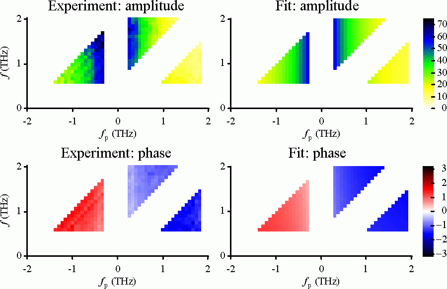
Fig. 7.
Spectra of transient conductivity Δσ of radiation-damaged silicon on sapphire in the two-dimensional frequency domain. Left panels: experimental results, right panels: Drude model of conductivity in the two-dimensional frequency domain. Bottom panels: amplitude of the conductivity |Δσ| in Ω·m−1·THz−1, bottom panels: phase arg(Δσ) in radians. The lifetime of electrons was 420 fs and the electron relaxation time is shorter than 50 fs.
Ultrafast opto-terahertz modulators
Terahertz technology is a research field which has a growing impact e.g. on medical, space and defence industries. As future short-range indoor communication systems may be designed for the sub-terahertz or terahertz range, one can expect a growing emphasis put on the manipulation of both guided and freely propagating terahertz beams by means of agile switches, modulators, and phase shifters controlled either optically or electronically. Optically controlled terahertz switches or filters are of particular interest as they are in principle able to achieve ultrahigh speeds.
High-resistivity semiconductors show a big potential for opto-terahertz coupling. In the ground state, they are transparent and dispersion free for terahertz radiation. Upon optical illumination, free carriers are generated: they exhibit a strong interaction with terahertz radiation, which can be tuned by the illumination.
We have demonstrated that photoexcitation of teh surface of bare GaAs can lead to the tuning of the THz reflection between antireflective (R ≅ 3 %) and highly reflective (R ≅ 85 %) regimes, depending on the excitation intensity [17], Fig. 8).
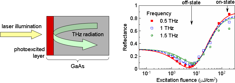
Fig. 8. Left panel: scheme of the opto-terahertz switch based on a photo-excited GaAs wafer with one illuminated surface. Right panel: measured reflectance as a function of excitation fluences for frequencies 0.5, 1.0 and 1.5 THz (the excitation wavelength was 800 nm). Points represent measured data while lines indicate results of modelling.
The use of a bare semiconductor wafer as an opto-terahertz switch is straightforward, but quite high excitation fluences are required for its operation. The controlling excitation fluence can be essentially decreased if the semiconductor is enclosed in a resonant structure—for example, it can play the role of a defect layer in a photonic crystal. In this case, the photonic structure can be designed in such a way that the terahertz electric field is spatially localized in the photo-excited layer, thus enhancing the interaction of the terahertz radiation with the photo-excited semiconductor surface [12, 17]. Such a device is typically narrow-band, since the localization of the electromagnetic field occurs only at the defect-mode frequency. We have shown that the dynamical response is determined by the resonator lifetime (switch-on time) and by the photocarrier lifetime (switch-off time).
An example of the investigated photonic-crystal-based modulator is shown in Fig. 9. It consists of a sequence of alternating layers of quartz and MgO (materials with high contrast of refractive indices at terahertz wavelengths and with high transparency in the visible optical region are required). The device exhibits a response time of ~200 ps, making it possible to construct an opto-terahertz modulator with modulation rates up to 5 GHz.
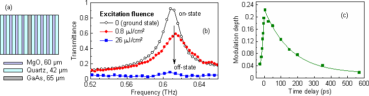
Fig. 9. (a) Scheme of the ultrafast photonic-crystal-based modulator. (b) Measured transmittance spectra for few excitation fluences. A modulation of 50 % can be achieved with excitation fluence as low as 0.8 µJ/cm2. (c) Measured dynamical response of the opto-terahertz modulator at the defect-mode frequency (0.606 THz). The switch-on time is ~20 ps while the switch-off time is ~200 ps and it is limited by the photo-carrier lifetime.
Ultrafast carrier dynamics in semiconductors
Microcrystalline silicon
Microcrystalline silicon is a complex semiconductor material, which drives attention of the companies producing solar cells, displays and other opto-electronics devices. It consists of large grains (hundreds of micrometers) embedded in amorphous silicon tissue (Fig. 10). Large grains are composed of small silicon grains with dimensions of ~20 nm.
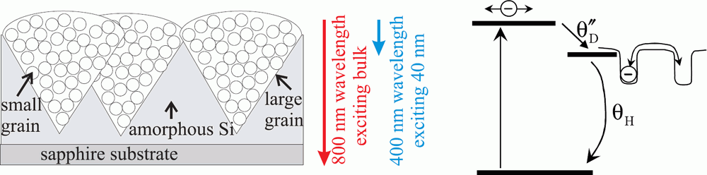
Fig. 10.
Left panel: structure of a microcrystalline silicon on a sapphire substrate. Large grains (~hundred nanometers) have conical shape with a cap and they consist of small grains (~20 nm). Large grains are surrounded by amorphous tissue. Small grains are assumed to be closely packed. Right panel: photoinitiated electron dynamics in microcrystalline silicon.
Using time-resolved THz spectroscopy, we have studied a set of samples with varying crystallinity (0 – 72 %). Two different wavelengths were employed for the photoexcitation: (i) 400 nm which excites only a thin surface layer allows to investigate surface properties, and (ii) 800 nm which creates a homogeneous excitation profile enables to study properties averaged over the entire film thickness. In addition, experiments have been carried out at various temperatures in order to elucidate transport mechanisms of electrons.
The nature of the probing radiation allows us to access local (intra-grain) transport properties. We identified two regimes of conduction. Shortly after photoexcitation, the photogenerated carriers are hot and they exhibit a band-like transport within the small grains. Within θ″D ~ 0.6 ps, the hot carriers fall into shallow states on small grain boundaries (Fig. 10). On longer time scales, these carriers move through hopping between the localized states. Finally, the charge carriers either recombine or become captured in deep traps at large grain boundaries [9, 15].
Ultrarychlé polovodiče
Photoconductive materials with subpicosecond response times have a wide range of applications in optoelectronics as terahertz emitters, photoswitches, and photodetectors. Their dynamic responsivity depends mainly upon the carrier lifetime, the carrier mobility and the dark resistivity. The group of interesting ultrafast photoconductive materials includes e.g. radiation-damaged silicon-on-sapphire or low-temperature grown GaAs. Short carrier lifetimes are achieved by a generation of a large density of defects either through an ion bombardment or using specific deposition conditions. The corresponding defect energy levels in the band gap then act as carrier traps or recombination centres. The main problem associated with the responsiveness of such materials is that their free-carrier mobility and their resistivity can be significantly reduced comparing to the state without defects. A detailed understanding of the mechanisms of the ultrafast response is thus a crucial point that can allow to optimise the elaboration technology and to control the properties.
In0.53Ga0.47As a InP bombardované ionty Br+
Particularly interesting optoelectronic properties are produced by bombarding semiconductors by ions with a high initial energy which generates only host-atom displacements near the wafer surface while ions used for the bombardment are implanted a few microns below the wafer surface. Heavy-ion irradiation creates defect clusters in addition to the point defects.
We studied In0.53Ga0.47As and InP irradiated by 11 MeV Br+ ions. Our optical excitation wavelength of 800 nm is absorbed within a sub-micron surface layer. This enabled us to investigate three kinds of samples: (i) bare irradiated InP wafers and (ii) bare irradiated In0.53Ga0.47As films – these contain only host-atom displacements and no implanted Br atoms [B-samples] within the photoexcited layer, and (iii) irradiated InP wafers initially covered with a protective 3 µm-thick In0.47Ga0.53As layer – this layer was etched after irradiation so that we could look into a 3 µm depth where the Br atoms are implanted [E-samples]. Using optical pump—THz probe spectroscopy, we determined the electron trapping times and mobilities as a function of the irradiation dose (Fig. 11). We found that the transport properties are controlled only by the density of host-atom displacements while the Br atom implantation has no significant influence. In the most irradiated sample it was observed that the electron lifetime is as short as 200 fs and that the mobility remains rather high even at the highest irradiation doses [6, 10].

Obr. 11.
Graf (a) doby záchytu elektronů τdecay a (b) pohyblivosti μ v závislosti na hustotě defektů nhost vzniklých posunutím vlastních atomů mřížky. Čárkovaná čára v části (a) ukazuje trend dat (τdecay je přímo úměrné 1/nhost), čárkovaná křivka v části (b) ukazuje odhad pohyblivosti na základě Matthiessenova pravidla.
Low-temperature-grown GaAs
Using THz emission spectroscopy, we have determined carrier lifetimes and mobilities in a set of samples grown at different temperatures. Sub-picosecond lifetimes and very high mobilities (~2500 cm2V−1sV−1) have been found in all the samples (Fig. 12) [25].
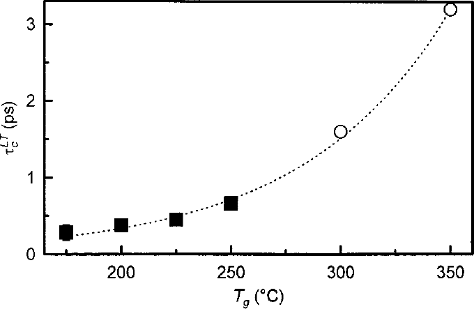
Fig. 12.
Lifetimes of low-temperature-grown GaAs as a function of growth temperature. The empty points were taken from [Appl. Phys. Lett. 70, 2419 (1997)].
Non-linear properties of GaAs
Optical pump–THz probe spectroscopy is also useful for measuring nonlinear optical properties of semiconductors [22]. When amplified pulses at 800 nm illuminate the surface of bulk GaAs, both one- and two-photon excitation of valence electrons occurs and their corresponding concentrations are functions of depth on the scale of several µm. By means of THz probing from inside the sample, it is possible to measure the depth of the photoexcited layer – the method is to a certain extent analogous to time-of-flight spectroscopy. By this method, we have determined, for the first time, the two-photon absorption coefficient β of GaAs at excitation wavelength of ~810 nm.
Dynamics of non-resonantly induced plasma in gases
Another recent extended study using the optical pump—THz probe spectroscopy focused on the mechanism of photoionisation and ultrafast dynamics of the plasma created by photoexcitation in molecular oxygen and nitrogen [11, 16]. We have shown that the ionisation mechanism is multiphoton absorption in case of 400 nm excitation and strong-field effect for the 800 nm pump.
Optical rectification at metal surfaces
Recently, we have demonstrated a new possibility of generating pulsed THz radiation by means of optical rectification at metal surfaces [18, 21]. This phenomenon is due to an effective second-order non-linear susceptibility tensor χijk which vanishes in the bulk of the (centrosymmetric) metals, but is non-zero at the surface and just below due to the absence of translational symmetry. This has been known for decades, as second-harmonic generation at metal surface is well-known. By contrast, optical rectification at metals was not observed until recently. With amplified pulses, we were able to achieve a peak intensity of the electrical field of 4 kV/cm, comparable to that obtained with non-linear crystals.
Related publications
| [1] |
C. Ponseca, H. Němec, N. Vukmirović, S. Fusco, E. Wang, M. Andersson, P. Chábera, A. Yartsev, and V. Sundström,
Electron and hole contributions to the terahertz photoconductivity of a conjugated polymer:fullerene blend identified,
J. Phys. Chem. Lett. 3, 2442 (2012).

|
|---|---|
| [2] |
Z. Mics, H. Němec, I. Rychetský, P. Kužel, P. Formánek, P. Malý, and P. Němec,
Charge transport and localization in nanocrystalline CdS films: a time-resolved terahertz spectroscopy study,
Phys. Rev. B 83, 15 5326 (2011).
|
| [3] |
H. Němec, P. Kužel, and V. Sundström,
Charge transport in nanostructured materials for solar energy conversion studied by time-resolved terahertz spectroscopy,
J. Photochem. Photobiol. A 215, 123 (2010).
|
| [4] |
H. Němec, J. Rochford, O. Taratula, E. Galoppini, P. Kužel, T. Polívka, A. Yartsev, and V. Sundström,
Influence of the electron-cation interaction on electron mobility in dye-sensitized ZnO and TiO2 nanocrystals: a study using ultrafast terahertz spectroscopy,
Phys. Rev. Lett. 104, 19 7401 (2010).
|
| [5] |
H. Němec, P. Kužel, F. Kadlec, D. Fattakhova-Rohlfing, J. Szeifert, T. Bein, V. Kalousek, and J. Rathouský,
Ultrafast terahertz photoconductivity in nanocrystalline mesoporous TiO2 films,
Appl. Phys. Lett. 96, 06 2103 (2010).
|
| [6] |
J. C. Delagnes, P. Mounaix, H. Němec, L. Fekete, F. Kadlec, P. Kužel, M. Martin, and J Mangeney,
High photocarrier mobility in ultrafast ion-irradiated In0.53Ga0.47As for terahertz applications,
J. Phys. D 42, 19 5103 (2009).
|
| [7] |
H. Němec, H.-K. Nienhuys, E. Perzon, F. Zhang, O. Inganäs, P. Kužel, and V. Sundström,
Ultrafast conductivity in a low-band-gap polyphenylene and fullerene blend studied by terahertz spectroscopy,
Phys. Rev. B 79, 24 5326 (2009).
|
| [8] |
H. Němec, P. Kužel, and V. Sundström,
Far-infrared response of free charge carriers localized in semiconductor nanoparticles,
Phys. Rev. B 79, 11 5309 (2009).
|
| [9] |
L. Fekete, P. Kužel, H. Němec, F. Kadlec, A. Dejneka, J. Stuchlík, and A. Fejfar,
Ultrafast carrier dynamics in microcrystalline silicon probed by time-resolved terahertz spectroscopy,
Phys. Rev. B 79, 11 5306 (2009).
|
| [10] |
H. Němec, L. Fekete, F. Kadlec, P. Kužel, M. Martin, J. Mangeney, J. C. Delagnes, and P. Mounaix,
Ultrafast carrier dynamics in Br+-bombarded InP studied by optical pump — terahertz probe spectroscopy,
Phys. Rev. B 78, 23 5206 (2008).
|
| [11] |
Z. Mics, P. Kužel, P. Jungwirth, and S. E. Bradforth,
Photoionization of atmospheric gases studied by time-resolved terahertz spectroscopy,
Chem. Phys. Lett. 465, 20 (2008).
|
| [12] |
L. Fekete, F. Kadlec, H. Němec, and P. Kužel,
Fast one-dimensional photonic crystal modulators for the terahertz range,
Opt. Exp. 15, 8898 (2007).
|
| [13] |
P. Kužel, F. Kadlec, and H. Němec,
Propagation of terahertz pulses in photoexcited media: Analytical theory for layered systems,
J. Chem. Phys. 127, 02 4506 (2007).
|
| [14] |
L. Fekete, F. Kadlec, P. Kužel, and H. Němec,
Ultrafast opto-terahertz photonic crystal modulator,
Opt. Lett. 32, 680 (2007).
|
| [15] |
L. Fekete, H. Němec, F. Kadlec, P. Kužel, J. Stuchlík, A. Fejfar, J. Kočka,
Carrier dynamics in microcrystalline silicon studied by time-resolved terahertz spectroscopy,
J. Noncryst. Solids 352, 2846 (2006).
|
| [16] |
Z. Mics, F. Kadlec, P. Kužel, P. Jungwirth, S. E. Bradforth, V. A. Apkarian,
Nonresonant ionization of oxygen molecules by femtosecond pulses: Plasma dynamics studied by time-resolved terahertz spectroscopy,
J. Chem. Phys. 123, 10 4310 (2005).
|
| [17] |
L. Fekete, J. Y. Hlinka, F. Kadlec, P. Kužel, and P. Mounaix,
Active optical control of the terahertz reflectivity of high-resistivity semiconductors,
Opt. Lett. 30, 1992 (2005).
|
| [18] |
F. Kadlec, P. Kužel, J.-L. Coutaz,
Study of terahertz radiation generated by optical rectification on thin gold films,
Opt. Lett. 30, 1402 (2005).
|
| [19] |
H. Němec, F. Kadlec, S. Surendran, P. Kužel, and P. Jungwirth
Ultrafast far-infrared dynamics probed by terahertz pulses: A frequency domain approach. I. Model systems,
J. Chem. Phys. 122, 10 4503 (2005).
|
| [20] |
H. Němec, F. Kadlec, C. Kadlec, P. Kužel, and P. Jungwirth
Ultrafast far-infrared dynamics probed by terahertz pulses: A frequency domain approach. II. Applications,
J. Chem. Phys. 122, 10 4504 (2005).
|
| [21] |
F. Kadlec, P. Kužel, and J.-L. Coutaz,
Optical rectification at metal surfaces,
Opt. Lett. 29, 2674 (2004).
|
| [22] |
F. Kadlec, H. Němec, and P. Kužel,
Optical two-photon absorption in GaAs measured by optical-pump terahertz-probe spectroscopy,
Phys. Rev. B 70, 12 5205 (2004).
|
| [23] |
F. Kadlec, C. Kadlec, P. Kužel, P. Slavíček, and P. Jungwirth,
Optical pump-terahertz probe spectroscopy of dyes in solutions: Probing the dynamics of liquid solvent or solid precipitate?,
J. Chem. Phys. 120, 912 (2004).
|
| [24] |
H. Němec, F. Kadlec, and P. Kužel,
Methodology of an optical pump-terahertz probe experiment: An analytical frequency-domain approach,
J. Chem. Phys. 117, 8454 (2002).
|
| [25] |
H. Němec, A. Pashkin, P. Kužel, M. Khazan, S. Schnüll, and I. Wilke,
Carrier dynamics in low-temperature grown GaAs studied by terahertz emission spectroscopy,
J. Appl. Phys. 90, 1303 (2001).
|
| poslední změna 22. srpna 2012 | (úvodní stránka) |
|---|